Latchup
Latchup is a condition when the parasitic BJTs turn on to short the power supply through the substrate of the device. The current is limited by the substrate resistance alone.
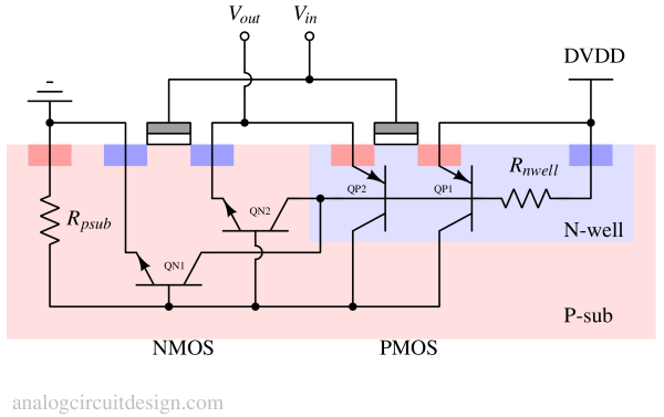
In a CMOS process where every device is built over a common p-substrate, there are parasitic BJTs that form a network apart from main CMOS devices.
The PNPN structure
For latchup, presence of PNPN structure is must. To identify the possibility of latchp, it is required to identify any PNPN structure getting formed.
It doesn't mean that presence of PNPN structure will always cause latchup. It depends certain conditions which we will discuss in following sections.

As mentioned in Fig 1, a substrate current goes through the substrate resistance Rpsub causing the VBE of lateral NPN to rise. This rise in VBE of lateral NPN causes an exponential collector current which results in a drop in VBE of vertical PNP. The drop in VBE of vertical PNP pushes more current through Rpsub which again rises the VBE of lateral NPN. This becomes a positive feedback loop which increases the current till it is limited to Vsup/(Rpsub+Rnwell).
Why the parasitic PNPN structure is not always in a latchup?
Now let's try to locate these parasitic BJTs in an actual CMOS inverter cross-section.

$$\text{LG} = \cfrac{\beta{}_{pnp}\beta{}_{npn}R_{psub}R_{nwell}}{\left(R_{psub}+r_{pi{},npn}\right)\left(R_{nwell}+r_{pi{},pnp}\right)}$$
This loop gain (LG) of the positive feedback circuit should be less than 1 for the circuit to not latch up. At low currents β is very low. This makes sure that loop gain is less than 1. However, with circuits having large substrate currents or high substrate resistances, there is chance that the current becomes high enough to make β more than 1.
Latchup prevention in integrated circuits
There are primary 2 reasons for latch-up to occur :
- High substrate resistance.
- High substrate coupling current.
Substrate resistance depends on how far supply and ground terminals (with the substrate) are located. The more the distance, the higher is the substrate resistance. So, it is required to put supply contacts as specified by the foundry. By putting more such terminals create parallel paths for current to flow. This makes the resistance to reduce and hence lower the VBE voltage.
Substrate current coupling can be minimized by minimizing any substrate stray current. It is done by putting a guard ring tied to appropriate supply voltage in the substrate so that the stray substrate current does not go outside the ring. Now the stray current generated from the circuit goes to the supply (because of low resistance path) rather than coupling to a parasitic BJT of nearby circuit.