MOSFET
MOSFETs are types of Field effect transistors (FETs) where the control terminal is isolated from the conduction channel using an oxide layer (insulator). The control terminal cannot conduct current in any condition. Processes with both NMOS and PMOS are called Complementary MOSFETs (CMOS).
JFET vs MOSFET
In JFETs, the control terminal is not isolated from the channel. If forward biased, the gate terminal conducts significant current. That is why in JFET, to minimize gate current, source-gate junction is reversed biased. In contrast, the current in MOSFET is always zero in any condition due to insulation provided by gate-oxide.
Types of MOSFETs
MOSFET is FET with an insulated Gate (usually silicon dioxide) that prevents DC current from flowing into the Gate terminal, resulting in extremely high input impedance. MOSFETs are the most popular transistors.
flowchart TD
    A[FET] --> B[JFET]
    A --> C[MOSFET]
    C --> D[Enhancement Mode]
    C --> E[Depletion Mode]
    B --> F[Depletion Mode]
    F --> G[P-channel]
    F --> H[N-channel]
    D --> I[P-channel]
    D --> J[N-channel]
    E --> K[P-channel]
    E --> L[N-channel]
Operating modes
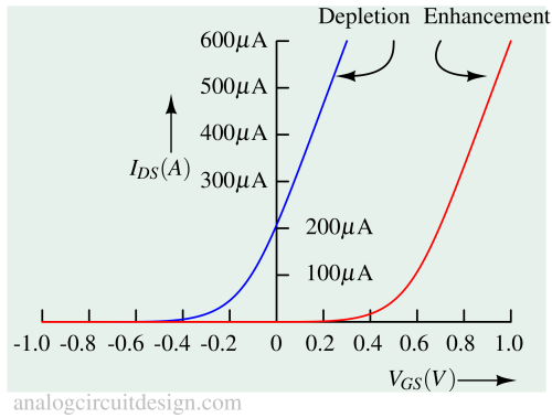
Enhancement mode
In Enhancement mode, the device is normally-off (non-conducting) when the Gate-Source voltage VGS is zero. An electric field must be applied via the Gate to "enhance" or grow a conductive channel between the Source and Drain. Enhancement mode MOSFETs are most common.
Depletion mode
In Depletion mode, the device is normally-on when VGS is zero. The channel is physically present by default. To turn the device off, a voltage must be applied to the Gate to "deplete" the channel of charge carriers, effectively pinching off (or choking) the channel.
Channel Types
Channel is formed in the body to conduct current. There are two types of channel, N-channel and P-channel :
- N-channel (NMOS) - The channel formed between the source and drain is of N-type after inversion in the body. The body is made of P-type material. N-channel MOSFET is also called NMOS. More about NMOS : N-Channel MOSFET (NMOS)
- P-channel (PMOS) - The channel formed between the source and drain is of P-type after inversion in the body. The body is made of N-type material. P-channel MOSFET is also called PMOS. More about PMOS : P-Channel MOSFET (PMOS)
The differences are tabulated below :
| Channel Type | Body doping | Source and Drain doping | Charge Carrier | On-state Gate-Source voltage |
|---|---|---|---|---|
| N-channel (NMOS) | P-type | N-type | Electrons (Negative charge) | Positive gate-source voltage |
| P-channel (PMOS) | N-type | P-type | Holes (Positive charge) | Negative gate-source voltage |
MOSFETs vs BJTs
FETs are different from BJTs. In BJTs, barrier voltage is lowered and thermal energy causes the charge carriers to flow. In FETs, an electric field enhances or deplete the charge carrier density in the conduction path. More differences are listed below :
| MOSFETs | BJTs | |
|---|---|---|
| Flicker noise | Worse than BJTs | 10X better than MOSFETS |
| Matching | Worse than BJTs | Better than MOSFETs |
| Transconductance (gm) | Low gm for a given current (proportional to √ID) | Higher gm for a given current (proportional to IC) |
| Speed | Can achieve very high speed to due very small size | Cannot be scaled to low to get high speed as MOSFET |
| Scalability | Highly scalable | Not very scalable as MOSFET |
| Digital circuits | Highly favorable for digital circuits due to negligible off-current | Not favorable for digital circuits due to high off-current (usually ~1uA per transistors) |
| Noise contribution type | Thermal noise and Flicker noise | Shot noise and Flicker noise |
| Reliability | Due to possibility of gate-oxide breakdown, it is less reliable | Due to no gate-oxide, it is highly reliable |
| Suitability as switch | Highly suitable due to almost zero off-state current | Not suitable due to non-zero off-state current |
| Input resistance | Infinite | rπ |
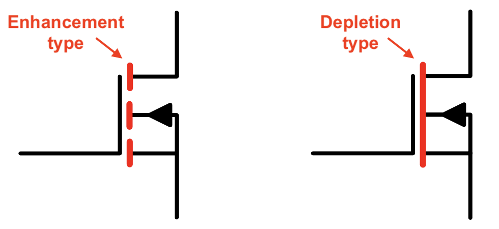
Symbol and Terminals
MOSFET symbols depict a three or four-terminal device (Gate, Drain, Source, Body) with a channel line separating the drain and source. Sometimes arrow is indicated on the body terminal (popular in power electronics) and sometimes the arrow is indicated on the source terminal (popular in analog signal processing circuits). Arrow indicates direction of on-current.

Outward arrow at source terminal represents an N-channel MOSFET and in-ward arrow at source terminal represents a P-channel MOSFET.
![]()
Outward arrow at body terminal represents an N-type body meaning P-channel MOSFET. In-ward arrow at body means P-type body meaning an N-channel MOSFET.
![]()
In Digital circuits, the arrow sign is omitted. Instead a dot sign is used to differentiate between NMOS and PMOS. PMOS has a dot sign at the gate while NMOS does not have it. Body and source are usually shorted together in digital circuits so there is no separate body terminal.
Construction
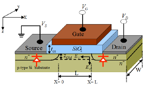
MOSFET has following important components:
- Gate : Controls the electric field in the channel which enhances or deplete the conduction in the conduction channel.
- Source : From this terminal, the majority charge carriers enters the conduction channel. The source terminal is one of the 2 terminals across the conduction channel.
- Drain : From this terminal, the majority charge carriers exit the conduction channel. The drain is the other of the 2 terminals across the conduction channel.
- Bulk (or body) : This terminal is used as a reference terminal. Bulk voltage should always be lower than source voltage. Usually it is tied with the source terminal or the lowest potential in the circuit.
- Channel : The channel is the conductive path between the source and drain, formed by an inversion layer of charge carriers (electrons for N-channel, holes for P-channel). The inversion layer is created by the gate voltage, allowing current flow, with its conductivity controlled by that gate voltage.
- Gate oxide (SiO2) : The gate oxide of a MOSFET is a thin, insulating layer—typically SiO2 that separates the gate electrode from the conductive channel. It prevents DC current flow into the channel through gate while still allowing gate to control the channel's conduction.
- Body diode : Body diode are the parasitic diodes formed by the MOSFET's internal P-N junction between the source, drain and body.
Principle of operation
In MOSFET, the conduction between 2 terminals (Drain and Source) is controlled through a voltage applied to another terminal (Gate).
Enhancement type N-channel MOSFET
Enhancement MOSFETs, are in an off-state at gate-to-source voltage (VGS) of 0V and turns on after VGS > VTH. Enhancement MOSFETs (both N-channel and P-channel) are the most popular.
Depletion type N-channel MOSFET
Depletion MOSFETs, unlike enhancement MOSFETs, are in an on-state even at 0 V of gate-to-source voltage (VGS). This feature makes them suitable for using as a constant current source as well as in other ways.
Threshold Voltage
The threshold voltage VTH of a MOSFET is the minimum gate-to-source voltage required to create a conducting inversion channel. It is normally assumed that the bulk of the MOSFET is connected to source. However, sometimes the bulk and source are in different potentials (VSB ≠ 0). VSB is called “body bias”. Note that the body and source are always reversed bias. VSB is the reverse bias magnitude. The threshold voltage with body bias can be calculated as :
$$V_{TH}=V_{TH0}+\gamma{}\left(\sqrt{|2\phi{}_F+V_{SB}|}-\sqrt{|2\phi{}_F|}\right)$$
In this equation, VTH is the zero bias threshold voltage, γ is the body bias coefficient, and φF is :
$$\phi{}_F=\cfrac{kT}{q}\ln{\cfrac{N_A}{n_i}}$$
Where NA is the doping concentration in the substrate.
Example
Assume that VTH0=0.8V, γ=0.6 V1/2 , φF= 0.4V. Find VTH if VSB=2.5V
$$V_{TH}=V_{TH0}+\gamma{}\left(\sqrt{|2\phi{}_F+V_{SB}|}-\sqrt{|2\phi{}_F|}\right)$$
$$V_{TH}=0.8V+0.6\times{}\left(\sqrt{|2\times{}0.4+2.5|}-\sqrt{|2\times{}0.4|}\right)=0.8+0.55=1.35$$
Body bias increases threshold voltage. Threshold voltage is positive for normal NMOS and it is negative for PMOS.
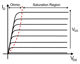
Operating Regions
In a MOSFET, a voltage is applied between the gate and the source terminals, and the resulting current flowing between the drain and source is measured. Different combinations of gate–source and drain–source voltages establish the electric field in the device and give rise to different regions of operation, such as cutoff, triode (linear), and saturation.
Cutoff Region
The above figure shows how VGS affects the flow of current through the MOSFET. In an enhancement-mode N-channel MOSFET, when there is no voltage applied between the gate and the source, no conduction channel is formed between the drain and the source. This condition is known as the cutoff region. In this operating region, the drain current is ideally zero, and the MOSFET behaves like an open switch, preventing current flow between the drain and source terminals.
Drain-Source current:
$$I_{DS}=0$$
Subthreshold Region
The subthreshold region (or weak inversion) in a MOSFET occurs when the gate-to-source voltage VGS is below the threshold voltage VTH, causing a small, exponential leakage current to flow between the drain and source. It enables ultra-low-power operation essential for battery-operated devices.
$$I_{DS}\simeq{}\mu{}_nC_{ox}\cfrac{W}{L}\left(\cfrac{kT}{q}\right)^2(n-1)\left(1-\lambda{}V_{DS}\right)e^{q\left\{V_{GS}-V_{TH}\right\}/nKT}\left(1-e^{-qV_{DS}/KT}\right)$$
Where λ is the Early effect parameter and,
$$n\simeq{}\left\{1+\cfrac{1}{C_{ox}}\sqrt{\cfrac{\epsilon{}_{si}qN_A}{2\{-2\phi{}_p-V_{BS}\}}}\right\}$$
Linear, Triode or Ohmic Region
The MOSFET linear region, often called the triode region or ohmic region, occurs when VGSVTH (channel exists) and VDS < VGS-VTH (no pinch-off). In this region, the MOSFET behaves as a voltage-controlled resistor, where the drain current ID varies linearly with small drain-source voltage VDS.
Drain-Source current:
$$I_{DS}=\mu{}_nC_{ox}\cfrac{W}{L}\left[(V_{GS}-V_{TH})V_{DS}-\cfrac{V_{DS}^2}{2}\right]$$
If VDS << VGS - VTH, the equation can be simplied to:
$$I_{DS}\simeq{}\mu{}_nC_{ox}\cfrac{W}{L}(V_{GS}-V_{TH})V_{DS}$$
In the simplified equation, the drain-source current is proportional to drain-source voltage. The channel "on" resistance can be derived from the above equation:
$$R_{on}=\cfrac{V_{DS}}{I_{DS}}\simeq{}\cfrac{1}{\mu{}_nC_{ox}\cfrac{W}{L}(V_{GS}-V_{TH})}$$
The "on" resistance of the channel reduces with higher gate-source voltage.
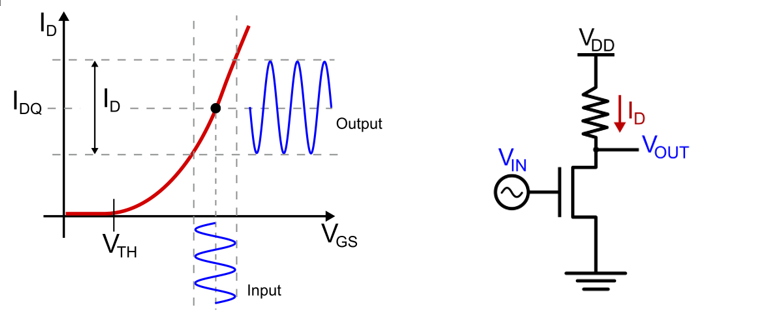
Saturation region
The saturation region in a MOSFET occurs when the drain-to-source voltage VDS exceeds the overdrive voltage VGS-VTH, causing the conductive channel to pinch off near the drain. In this region, the drain current IDS saturates becoming relatively independent of VDS and acts as a constant current source controlled by the gate voltage.
Drain-Source current:
$$I_{DS}=\cfrac{\mu{}_nC_{ox}}{2}\cfrac{W}{L}\left[V_{GS}-V_{TH}\right]^2$$
Transcondutance (gm) is defined in the saturation region of the MOSFET. Transconductance signifies the sensitivity of the output drain current IDS to changes in the input gate-source voltage VGS, acting as a measure of voltage-to-current amplification. The unit of measurement is Siemens (S). It is derived by taking the partial derivative of IDS with respect to VGS at a constant drain-source voltage.
$$g_m=\frac{\partial I_{DS}}{\partial V_{GS}}$$ $$g_m=\sqrt{2\mu{}_nC_{ox}(W/L)I_{DS}}$$
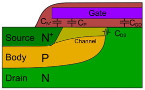
MOSFET parasitic components
MOSFETs contain unintended parasitic componets for example capacitances, resistances, and a body diode. Major capacitances include CGS (gate-source), CGD (gate-drain/Miller), and CDS (drain-source), which create non-linear, voltage-dependent input/output capacitances. These, along with parasitic gate/source inductance and body-diode capacitance, cause overshoot and ringing.
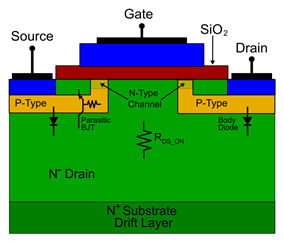
Key Parasitic Components:
-
Gate-Source Capacitance CGS: Formed by the overlap of the polysilicon gate and the source/channel region, independent of applied voltage.
-
Gate-Drain Capacitance CGD (Miller Capacitance): Consists of the gate-to-silicon oxide capacitance and the overlap with the JFET region. This is highly non-linear and limits switching speed. It creates a "Miller plateau" during switching, extending turn-on/off times and increasing losses.
-
Drain-Source Capacitance CDS: Associated with the PN junction of the intrinsic body diode (substrate-to-drain).
-
Parasitic Body Diode: An inherent PN junction between the drain and source which turns on even when gate-source voltage is zero. This diode is useful in motor drives and switching regulator applications. The body diode's forward voltage drop (~0.7V-0.9V) and reverse recovery charge Qrr can lead to high losses.
-
Parasitic Inductance LG,LD,LS: Caused by bond wires and package leads, typically in the nanohenry range, leading to voltage spikes and oscillations.
Applications
- Switching Power Supplies (SMPS): MOSFETs are used in laptop adapters, phone chargers, and DC-DC converters to efficiently convert and regulate voltage.
- Motor Control & Automotive: They control motor speed and torque via Pulse-Width Modulation (PWM) in robots, electric vehicles, and power steering systems.
- Digital Circuits (Logic Gates): Billions of MOSFETs form the core of microprocessors and memory chips (RAM), using CMOS technology for low power consumption.
- Renewable Energy Systems: Used in solar inverters and wind energy converters to manage power conversion and increase efficiency.
- Amplifiers: Due to high input impedance, MOSFETs are used in audio equipment, radio frequency (RF) circuits, and signal processing.
- Protection Circuits: Used in reverse polarity protection and soft-start circuits to protect delicate components.