MOSFET circuit model
In this article, a linear model of MOSFET will be discussed. Real devices are non-linear in nature. Analysis of nonlinear devices is prohibitively complicated. To simplify the analysis and understanding, it is converted to a linear model which is reasonably accurate for small signals.
Transconductance
In active/pinch-off region, MOSFET behaves as a voltage-controlled current source (VCCS). It is because the field in the channel is completely controlled by the voltage on the gate. The output current depend on the input voltage (V_{GS}) only and does not depend on the output voltage (V_{DS}) (it depends but very less in comparision to input voltage). We use term called "transconductance" to represent the magnitude of VCCS.
Transconductance,
$$g_m = mu{}C_{ox}\cfrac{W}{L}\left(V_{GS}-V_T\right)$$
or
$$g_m = \cfrac{2I_D}{V_{GS}-V_T}$$
Small Signal Model
Low frequency model
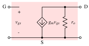
The small signal model is a linear model of a real MOSFET. It is valid for small voltage/current swing near the DC bias po\int. However it is very effective to predict large signal (including some nonlinearity) behavior of a circuit.
The same small signal model is applicable for both PMOS and NMOS.
High frequency model
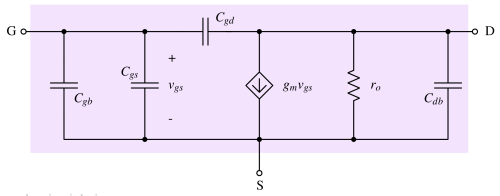
Amplifier configurations (2-ports models)

There are 3 small signal two-port models used for MOSFET known as:
- Common Source (CS)
- Common Gate (CG)
- Common Drain (CD)
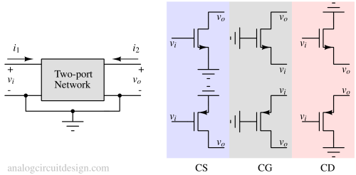
These 3 configurations form the building blocks of amplifiers and many other analog electronics systems. Various permutations of these help in building very large analog systems.
Common source (CS)
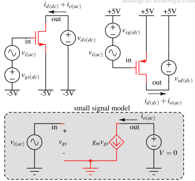
In this configuration, the source is tied to a DC voltage. No signal is provided at the source. The input voltage signal is provided to the Gate. Output is captured as a current at the Drain terminal because output (Drain terminal) acts as a current source. To measure the current at the Drain, the Drain is held at a constant voltage Vo(dc). If the output current is flown through a large resistance, a large voltage gain can be obtained.
This configuration can be termed a voltage-controlled current source (VCCS) because the input is a voltage and the output is a current.
Common gate (CG)
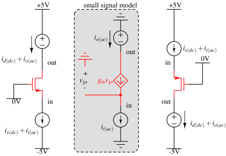
In this configuration, the Gate terminal is tied to a DC voltage. No signal is given to the Gate terminal. The input signal is provided at the Source terminal in form of current because input impedance is low. Output is captured as a current at the Drain terminal because output impedance is very high.
This configuration behaves like a current-controlled current source (CCCS) because the input is a current and output is also a current.
Common drain (CD)
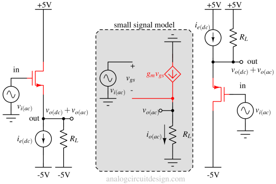
In this configuration, the Drain terminal is tied to a DC voltage. No signal is given to the Drain terminal. The input signal is provided at the Gate terminal in form of voltage because input resistance is almost infinite (except some capacitance which is of concern at high frequencies). Output is captured as the voltage at the Source terminal because output impedance is very low (so, Source is acting as a voltage source).
This configuration behaves like a voltage-controlled voltage source (VCVS) because the input is a voltage and the output is also a voltage. The voltage gain is usually ≤1.
What do we mean by “output is also a voltage”?
We mean that the output terminals maintain the desired voltage across a load without the voltage level getting too much attenuated. Output voltage is not attenuated only if the output resistance of the source is much lower than the load resistance (same as voltage divider concept of resistive network).
Small signal resistances
Input resistance
Since there is an oxide layer in series with gate and channel, the resistance is more or less infinite. There exist only capacitive impedances which will be discussed in the coming sections.
Output resistance (also called 'r-o')
Usually a MOSFET behave like current source if input is tied to constant DC voltage. Output current of ideal current source should remain constant with the voltage applied. However, this does not happen in BJT/MOS.
In reality, he output current rises with increases in collector-emitter voltage. This is because the the channel length reduces. This shrinks the channel length is called channel length modulation.
Small signal capacitances
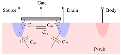
Gate-source capacitance - Cgs
Gate source capacitance represent the channel charge (C_{cc}) overlap capacitance (C_{ov}). The overlap capacitance is created due to overlap of gate polysilicon with source diffusion. This overlap capacitance depend on the width of the device.
In active/pinch-off region:
$$C_{gs} = C_{cc} + C_{ov}$$
$$C_{cc} = \cfrac{2}{3}C_{ox}WL$$
Source-bulk capacitance - Csb
This capacitance is mostly the depletion capacitance from source terminal to the body. If source and body are shorted then this capacitance go away. In large devices this source to body capacitance becomes very significant.
$$C_{sb} = \cfrac{C_{sb0}}{\left(1+\cfrac{V_{SB}}{psi{}_0}\right)^{1/2}}$$
Drain-bulk capacitance - Cdb
This capacitance is also the depletion capacitance from drain terminal to the body. Usually in active/pinch-off region, drain terminal is kept at a higher voltage which widens the depletion width and the capacitance reduces. In linear/triode region, when the drain voltage reduces, this capacitance can become significant.
$$C_{db} = \cfrac{C_{db0}}{\left(1+\cfrac{V_{DB}}{psi{}_0}\right)^{1/2}}$$
Gate-drain capacitance - Cgd
It is mainly the overlap capacitance created due to overlap of polysilicon of gate and diffusion region of drain.
$$C_{gd} = C_{ov}$$
Noise sources
Flicker noise
Flicker noise in MOSFET comes due to interface dangling charges which exist in the channel. These interface charges are just below the oxide and top of channel.
$$\cfrac{V_n^2}{\Delta{}f}=\cfrac{K}{WLC_{ox}f}$$
Thermal noise
Thermal noise is in MOSFET is modelled as :
$$\cfrac{i_d^2}{\Delta{}f}=4kT\gamma{}g_m$$
γ is named the excess noise factor and its value is 2/3 for a long-channel saturated transistor in strong inversion.
MOSFET Modeling & Theory
- MOSFET equations
- Small-signal model
- Large-signal model
- Square-law model
- Channel length modulation
- Body effect
- Short-channel effects
- Velocity saturation