NPN BJT Transistor
NPN is one of the types of BJT where the majority charge carriers are the electrons. The emitter is n-type (n+) doped, the base is p-type doped, and the collector is n-type doped. A positive base-emitter voltage turns on the transistor either in forward-active mode or saturation. In saturation, there is no gain. So, in saturation, the BJT is supposed to act as a turned-on switch.
Usually, an NPN transistor provides more advantages than a PNP transistor because :
- NPN has more β.
- NPN has lesser noise.
Construction of NPN transistor
In NPN, the P-type base is sandwiched between two N-type regions (emitter and collector).
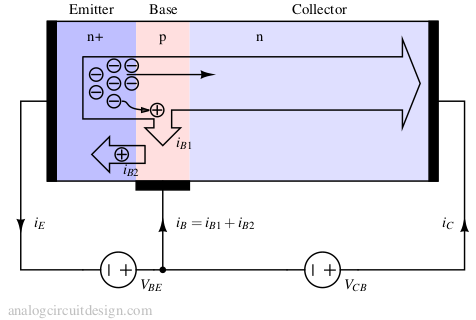
In the above Figure, the Emitter is constructed with n+ doping. This means that the doping concentration is higher than usual n-type doping. Also, there are usually 2 components of base current :
- Recombination of electrons in the base region with holes, iB1.
- Injection of electrons into the emitter region, iB2.
For first order analysis, considering the emitter injection current iB2 is sufficient.
A more realisitic contruction of NPN transistor
In actual NPN construction, the emitter-base-collector junction are not same as that shown in Fig. 1. The actual construction looks like Fig. 2.

It can be observed from the above figure that there exist a p-type (diffusion) channel between Emitter (n+) and Collector (n-epi). This is the base region. n+ and p+ regions are usually used to form contacts with metals and semiconductors so that it offers the least resistance. Emitter n+ contact itself acts as the emitter region. While the actual base region is below the emitter region, it is farther away from base contact.
Please note the transistor formed is now vertical in nature. It is because the emitter-base-collector lies vertically. Also, note that the physical distance between base contact and emitter is less in comparison with the PNP transistor. So, the base resistance (r_b) would be less.
Also, the contacts form a closed shaped when view from the top. This is to make sure that the resistances are less.

What are P-diff, N-epi, NBL, and PSUB?
P-diff region is a p-type diffusion region over the n-epi region. In NPN transistor, it is used to create the base region.
PSUB – An entire silicon wafer is doped with a p-type material which forms the base over which all other transistors will be manufactured.
NBL is a medium doped region that is also applied throughout the wafer so that it can be used for isolation purposes. One NBL region can be isolated from another NBL region using trench isolation. However, one PSUB region is not isolated from another. The reverse bias NBL and PSUB region does the isolation avoid problems like noise coupling, latchup, breakdown, etc.
N-epi is nothing but an N-type epitaxial layer. Epitaxy is a very controlled method to deposit one material over another material. Using this method, the depth and doping can be precisely controlled and kept uniform across batches of wafers. In discrete NPN, since there is no sharing of the substrate, the buried layer can be avoided.
Operation in forward-active region
Now, an NPN BJT in the forward-active region (as an amplifier) would be discussed. A similar theory is applicable for PNP as well.
The Emitter is the source of the majority charge carriers. It is also heavily doped so that it can release more charge carriers. In NPN, it is electrons that are the majority charge carriers and the emitter releases them when barrier voltage is lowered by making (\(V_{BE}\)) positive.
The Base terminal is used to control the barrier voltage of the p-n junction (base-emitter). When the barrier is lowered by making (\(V_{BE}\)) positive, electrons are diffused into the base. The width of the base region is designed to be narrow so that electrons don't get enough time to recombine. That is why most of the electrons pass the base region and enter the reverse-biased p-n junction of the base-collector. Still, some recombination happens at the base which causes base current. Probably the most undesirable feature of BJT is the base current. This lowers the input impedance of the BJT making it less suitable as a voltage-controlled amplifier.
The Collector terminal is used to bias the base-collector p-n junction in reverse bias such that a depletion region is formed. One important property of the depletion region that we learned in the photodiode article is that any mobile charge carriers generated or put in this region will get pulled towards opposite potentials. Therefore there are no mobile charge carriers in the depletion region. This means that the electrons are pulled towards positive potential and holes are pulled towards negative potential. That is why electrons that pass the base region without recombining get pulled by the collector terminal (which is connected to a more positive potential in comparison to the base in NPN).
The transistor/amplification action is achieved because the base width is very narrow (less recombination) and high emitter doping (less injection of holes in emitter).
Current-Voltage relationship of NPN transistor
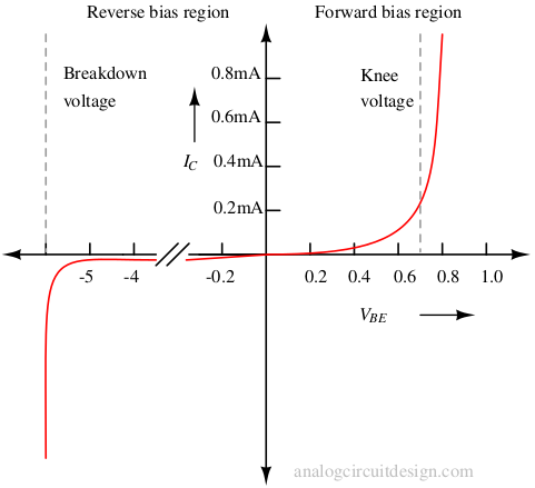
In NPN transistor during forward active mode, current-voltage relationship is :
$$I_C = I_S.\left[\exp{\left(\cfrac{V_{BE}}{V_t}\right)}-1\right].\left(1+\cfrac{V_{CE}}{V_A}\right)$$
$$I_B = \cfrac{I_C}{\beta{}}$$
where,
$$V_t = \cfrac{kT}{q}$$
$$V_A = \text{Early Voltage}$$
The above equation and plot \(\left(I_C,I_B\text{ vs. }V_{BE}\right)\) is used for design.
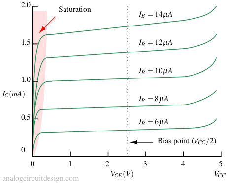
NPN in saturation or cut-off region
Getting the cut-off condition is straightforward. Because if \(V_{BE} < 0.5\text{V}\), then collector current becomes near zero.

For saturation, we should look into the 2N3904 datasheet. Particularly VCE(sat) and VBE(sat) specification is important in saturation case. VBE(sat) is usually the value of VBE when the transistor is in the saturation region.
We shall power-up (bias) the circuit at IC = 50mA. At this point IB = 5mA. We should note the VCE(sat) = 0.4V.
So values of Rb and Rc when the switch is open and therefore the transistor Q1 is in saturation,
$$R_b = \cfrac{V_{CC}-V_{BE(sat)}}{I_b} = \cfrac{5-0.65}{5\times{}10^{-3}}$$
$$\implies{} R_b = 870\Omega{}$$
$$R_c = \cfrac{V_{CC}-V_{CE(sat)}}{I_c} = \cfrac{5-0.4}{50\times{}10^{-3}}$$
$$\implies{} R_c = 90\Omega{}$$
NPN in forward-active region
In the forward-active region, we have the similar conditions as that of NPN.
$$I_B = \cfrac{I_C}{\beta{}}$$
β is called current gain. This value generally varies from 20 to 200 depending on the transistor. In the same transistor, it can vary with current density, as mentioned in the Gummel plot.
Also, there is another relation in forward-active region,
$$I_C = \alpha{}I_E$$
Also,
$$I_E = I_B + I_C$$
$$\implies{} \alpha{} = \cfrac{\beta{}}{1+\beta{}}$$
The relationship with (alpha{}) is not frequently used in comparision to β. It has been mentioned for the sake of completeness.

Our first step should be to bias the transistor in a DC operating point where it can act like an amplifier. For that we need to set the value of (Rb) and (Rc) properly.
Infinite capacitors denote that these act as short at anything except DC. Making them infinite make sure that any value of resistance does not form any filter with the capacitor and influence the AC frequency response. Capacitors make sure that the signal voltage does not affect DC bias conditions.
To achieve maximum output swing, we set \(V_{o(dc)} = V_{CC}/2\). We get following equations at DC,
$$R_c = \cfrac{V_{CC}-V_{o(dc)}}{I_C} = \cfrac{V_{CC}}{2I_C}$$
$$V_{CC}-R_bI_B-V_{BE} = 0$$
We chose VBE = 0.75V because it is midway of desired operating range in the Gummel plot. At VBE = 0.75V we find IB = 10μA using the Gummel plot. Assuming β=100, which gives IC = βIB = 1mA.
So, substituting the above values in the KCL equations.
$$R_C = \cfrac{5\text{V}}{2\times{}1\text{mA}} = 2.5\text{k}\Omega{}$$
$$R_B = \cfrac{V_{CC}-V_{BE}}{I_B} = 425\text{k}\Omega{}$$
Now the BJT is ready to do amplification. We shall learn more about amplification in the next article.
Also, we will discuss in detail PNP and NPN transistors specifically in a couple of articles. Basically, the PNP transistor has polarities and the direction of the current flipped.