PNP BJT Transistor
PNP is one of the types of BJT where majority charge carriers are the holes instead of electrons. The emitter is p+ doped, base is n doped and collector is p doped. A positive emitter-base voltage turns on the transistor either in forward-active mode or saturation. In saturation there is no gain, this mode is supposed to act as a turned-on switch.
Construction of PNP transistor
In PNP, the N-type base is sandwiched between two P-type regions (emitter and collector).
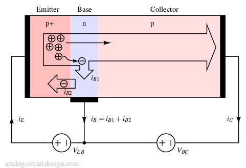
In the above Figure, the Emitter is constructed with p+ doping. This means that the doping concentration is higher than usual p-type doping.
Also, there are usually 2 components of base current :
- Recombination of holes in base region electrons, iB1.
- Injection of electrons into the emitter region, iB2.
For first order analysis, considering the recombination current is sufficient.
A more realistic contruction of PNP transistor
In actual PNP construction, the emitter-base-collector junction are not same as that shown in Fig. 1. The actual construction looks like Fig. 2.

It can be observed from the above figure that there exist a n-type (n-epi) channel between Emitter (p+) and Collector (p+). This is the base region. We can observe that the Emitter, Base and Collector are formed in a lateral (horizontal) manner. So, we often call these transistors as lateral transistors.
Also, there are multiple BJTs being formed. Multiple base contacts helps in reducing rb which improves the noise.
Why the base contact is not in-between Emitter and Collector?
It is because, if we put base contact (n+ diffusion) between emitter and collector, the physical distance between emitter and collector will increase. This will lead to a larger effective base area and the holes which are supposed to cross the base region will recombine with electrons in the base region. This will lead to a significant drop in current gain β.
That is why you can see that the base contact is placed outside the emitter-collector. However, there still exists the base region (n-epi) in between the emitter and collector.

What are N-epi, NBL, and PSUB? (Similar to NPN)
PSUB - An entire silicon wafer is doped with a p-type material which forms the base over which all other transistors will be manufactured.
NBL is a medium doped region that is also applied throughout the wafer so that it can be used for isolation purposes. One NBL region can be isolated from another NBL region. However, one PSUB region is not isolated from another. The reverse bias NBL and PSUB region avoid problems like noise coupling, latchup, breakdown, etc.
N-epi is nothing but an N-type epitaxial layer. Epitaxy is a very controlled method to deposit one material over another material. Using this method, the depth and doping can be easily controlled and kept uniform across batches of wafers.
In discrete PNP, since there is no sharing of the substrate, the buried layer can be avoided.
Current-Voltage relationship of PNP transistor
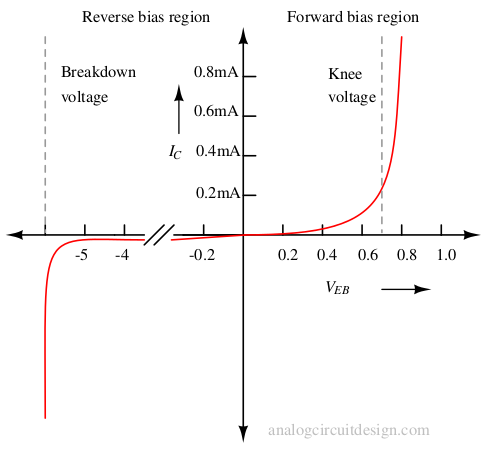
The current-voltage relationship of PNP and NPN is similar. In PNP transistor (in forward active mode) it is :
$$I_C = I_S.\left[\exp{\left(\cfrac{V_{EB}}{V_t}\right)}-1\right].\left(1+\cfrac{V_{EC}}{V_A}\right)$$
Where,
$$V_t = \cfrac{kT}{q}$$
VA is the Early voltage. These equations do not capture the breakdown and saturation region. These are good for forward bias, reverse bias (but not breakdown), and cut-off.
In the actual design of the circuit, the above equation is not used so frequently. It is because the above equation is dependent on IS and characterizing it is difficult and process-dependent. Most of the time Gummel's plot is used for design.
Also, for any region of operation, the below equation holds true, (it is just a KCL equation) :
$$I_E = I_C + I_B$$
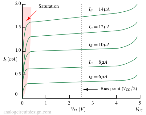
PNP in saturation or cut-off region.
PNP transistor is often used to power a relay on the high side of the supply as shown below. The switch can be another transistor from a microcontroller.

Getting the cut-off condition is straightforward. Because if VEB < 0.6V then collector current becomes near zero.
For saturation, we should look into the 2N3906 datasheet. Particularly VEC(sat) and VEB(sat) specification is important in saturation case. Sometimes datasheets use VBE to represent VEB in the case of PNP.
We shall power up (bias) the circuit at IC = 50mA. At this po\int IB = 5mA. We should note the VEC(sat) = 0.4V.
So values of Rb and Rc when the switch is open and therefore the transistor Q1 is in saturation,
$$R_b = \cfrac{V_{CC}-V_{BE(sat)}}{I_b} = \cfrac{5-0.65}{5times{}10^{-3}}$$
$$\implies{} R_b = 870,\Omega{}$$
$$R_c = \cfrac{V_{CC}-V_{CE(sat)}}{I_c} = \cfrac{5-0.4}{50times{}10^{-3}}$$
$$\implies{} R_c = 90,\Omega{}$$
Example : Level shifter using PNP transistor.
As an example of BJT as a switch, we shall design a level shifter that translates the digital signal from 5V levels to 3.3V levels using a PNP transistor.

The level shifter shown is better than a simple resistor divider because this PNP-based circuit has high pull-up strength (current). The pull-down strength is the same as a resistor divider network.
A better level shifter circuit exists which uses both NPN and PNP to provide both high pull-up and pull-down strength. That circuit is discussed in this article.
PNP in forward active region.
In forward-active region we have similar condition as that of NPN.
$$I_B = \cfrac{I_C}{b\eta{}}$$
Also, there is another relation in forward-active region,
$$I_C = alpha{}I_E$$
Also,
$$I_E = I_B + I_C$$
$$\implies{} alpha{} = \cfrac{b\eta{}}{1+b\eta{}}$$
The relationship with α is not frequently used in comparison to β. It has been mentioned for the sake of completeness.

To bias the above transistor in the forward-active region, we can refer 2N3906 datasheet. We wish to get maximum DC gain, so it is required to bias the transistor at maximum β. We find that at IC = 10mA when β is maximum at 100.
So,
$$I_B = \cfrac{I_C}{b\eta{}} = \cfrac{10,\text{mA}}{100}=100,mu{}\text{A}$$
$$V_{CC}-V_{EB}-I_BR_b=0$$
$$\implies{}5,\text{V}-0.7,\text{V}-100mu{}\text{A}.R_b=0$$
$$\implies{}R_b=43,\text{k}\Omega{}$$
We should set the Vo(dc) at mid-po\int (i.e., VCC/2) to get maximum output swing.
$$R_C = \cfrac{V_{o(dc)}}{I_C} = \cfrac{5/2,\text{V}}{10,\text{mA}} = 250,\Omega{}$$